A technology based on conventional MEMS technology has been devised for the fabrication of integrated photonic structures in the mid-infrared (IR) range. Using this technology, sensors for the characteristic mid-IR absorption in fluids can be realized, which allow to monitor the state of the fluids. This method is established and proven on the laboratory scale but has thus far not been widely implemented in production processes due to a lack of feasible devices (sensors). The newly devised technology solves this issue.
Modern production processes require ubiquitous presence of status information regarding the condition of machines and processing units as well as the composition of produced goods. The availability of these data is a crucial prerequisite for the implementation of concepts such as “industry 4.0”.
Fluids (liquids or gases) in a particular product as well as maintenance fluids play a major role in many production processes. This can be for instance a complex fluid in pharmaceutical of food production or a maintenance fluid such a lubrication oil of a machine. For process control but also for the detection of spurious states, the state of such liquids can be monitored. For the analysis of fluids, a variety of parameters are at hand. In analytical chemistry, infrared (IR) absorption is a particular useful method as it allows the efficient analysis of fluid composition. Here, specific molecules feature IR absorption at particular wavelengths in the IR range, such that every substance has a characteristic “fingerprint” in the IR spectrum. The mid-infrared range (MIR) is particularly interesting as most molecules feature characteristic absorption “fingerprints” there. However, integrated sensors tackling measurement in the MIR are scarcely available, yet. Established instruments used in analytical chemistry are most often not suitable for integration in processes as they are commonly bulky, expensive, and/or require manual maintenance or operation.
To tackle this problem, we devised a concept where we aim at measuring IR absorption at specific wavelength (which are of importance for a particular substance or process) rather than recording an entire spectrum. This is feasible, as for a particular application one is not confronted with the analysis of a completely unknown substance but rather variations of a basically known fluid have to be observed.
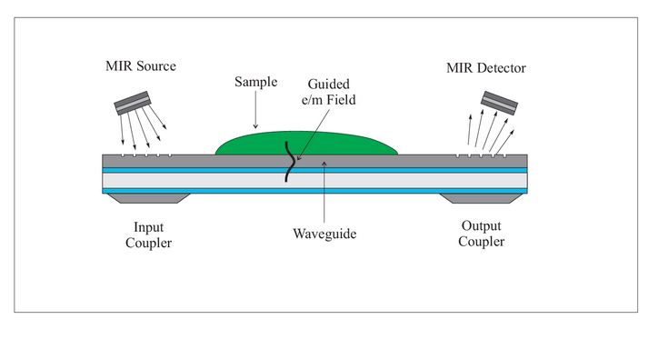
In our research we investigated and devised a technology, enabling the fabrication of MIR-absorption sensors utilizing MEMS (micro-electromechanical systems) technology, an established technology suitable for the realization of miniaturized mechatronic systems. The goal is to integrate a complete system, consisting of an IR emitter, a sensing element being in contact with the substance to be monitored, and a detector on a single chip (with dimensions in the mm-range). As sensing element an optical waveguide for MIR is used. Such a waveguide carries some of the guided electromagnetic wave outside of the waveguiding structure, i.e. in its vicinity (the so-called evanescent field). A fluid placed there would lead to characteristic absorption which can be detected by an attenuated signal in the detector. The structure also comprises elements yielding filtering of the MIR light to obtain the selected wavelengths. The latter are then fixed for a particular device but can be adapted to application by modifying the design of the device.
The technology has now been successfully devised, crucial IP has been patented or applied for patents. We are now at the stage of evaluating this technology using successfully fabricated demonstrator devices for sample applications and investigate the opportunities and the limits of this technology.
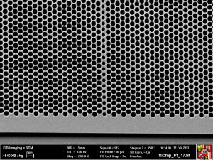
Fig.1: The concept of a MIR absorption sensor comprising a source, a waveguide as sensing element and a detector. The fluid to be investigated is placed in the evanescent field of the waveguide yielding characteristic attenuation of the guided IR wave (left). Scanning electron microscope (SEM) image of a waveguide. This particular design utilizes so called photonic crystal structures yielding a waveguiding effect for a particularly selected wavelength. The wave is guided along the line of intentional “defects” in the crystal structure (right).
Impact and effects
This technology will further the wide-spread application of the, on the laboratory scale, established successful IR-absorption measurement technology in applications, where thus far it could not be applied due to the lack of miniaturized and low-cost sensor devices. Typical branches will be production processes dealing with fluid products but also condition monitoring applications pertaining fluidic operation fluids.